Skip to content

Process Engineer – Research & Development

Dr.-Ing.Maram Abu‑Muhfouz

“From Materials Science to Industrial Process Development”

I connect thin-film technology, microstructure analysis and data-driven process optimisation – from the Max Planck Institute lab to scalable application.

  • Process Development
  • Microstructure Engineering
  • Phase Transformation
  • Material Characterization
  • Thin Film Fabrication

Düsseldorf, Germany

Logo Dr.-Ing. Maram Abu-Muhfouz

5+

years of research at the Max Planck Institute

3

languages: DE · EN · AR

15+

characterisation techniques

1st

place CTCN Climate Innovation Award

Professional Profile

Analytical. Systematic. Solution-driven.

Materials engineer with a PhD in Materials Engineering from RWTH Aachen and research at the Max Planck Institute for Sustainable Materials (formerly Max Planck Institute for Iron Research) in Düsseldorf. My focus is on fabricating and characterising thin films and on how process parameters define microstructure and, with it, material properties.

  • PhD in Materials Engineering

    RWTH Aachen – research at the Max Planck Institute, Düsseldorf

  • β-FeSi₂ thin films

    Sustainable absorber material made from earth-abundant elements for photovoltaics

  • Process development

    Parameter analysis and optimisation for DC/RF sputtering (PVD)

  • Microstructure & phases

    EBSD, ECCI, XRD, CL, FIB, APT – correlative characterisation

  • Problem-solving

    Analytical, systematic and data-driven

Project 1 · PhD Research

β-FeSi₂ Thin Films for Photovoltaics

A Study on the Microstructure Formation Mechanisms and Functional Properties of new β-FeSi₂-based Polycrystalline Thin Films for Photovoltaic Applications Using Correlative Electron Microscopy

Thesis summary

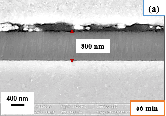
β-FeSi₂ thin films (~800 nm) were produced by controlled DC sputtering on stainless steel (304SS), Si (100) and sapphire Al₂O₃ (0001), to reach the best morphology, texture and spatial phase distribution.

  1. Process study

    A series of DC-PVD experiments on how combined sputtering parameters – and factors beyond them – drive morphology, texture formation, phase transformation and β-phase stability, including nucleation- vs. growth-controlled mechanisms.

  2. Correlative microscopy

    EBSD, XRD and EDS to monitor β-FeSi₂ formation; 2D EBSD maps on cross-sections and plan views for microstructure, phase distribution and texture; confocal laser microscopy for roughness.

  3. Challenge solved

    Classical Hough-transform indexing failed on complex tetragonal/orthorhombic phases, nano-sized grains and high defect density – so spherical indexing (SI) was used to identify the phases accurately.

Main findings

90% ± 10%

β-phase fraction on 304SS

45 ± 25 nm

uniform grain size

Ra = 32 nm

moderately smooth surface

(001)/(010)

sharp texture, shown for the first time

Optimal conditions: 1 h deposition · 12.12 nm/min · 500 °C substrate · 1 Pa – a continuous, high-quality film with good adhesion to 304SS.

SubstrateHighest β-phase fractionTexture
304SS90% ± 10% (1 h, 1 Pa, 500 °C)weakest; (010) poles strongest
Si (100)at 1 h, 0.5 Pa, 500 °Cstrongest; (010) poles strongest
Al₂O₃ (0001)98% ± 2%(001) peak strongest
Temperature: above 600 °C, Fe/Si interdiffusion at the interface sets in.
Chamber position: centre samples show a sharp fibre texture; outer samples show inclined fibres.

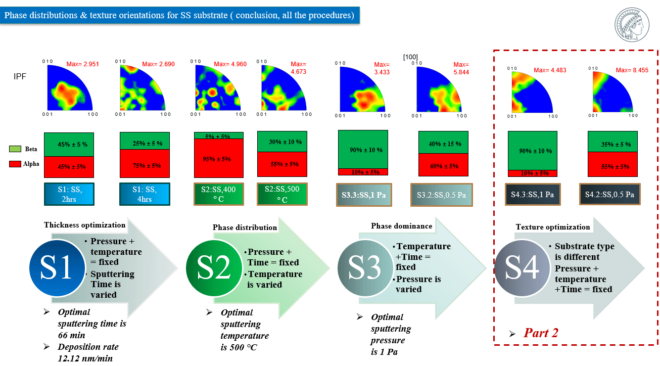
Optimisation route S1 → S4

Optimisation route S1 → S4
  1. S1

    S1 · Thickness

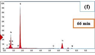
    Time varied → optimal 66 min, 12.12 nm/min

  2. S2

    S2 · Phase distribution

    Temperature varied → optimal 500 °C

  3. S3

    S3 · Phase dominance

    Pressure varied → optimal 1 Pa

  4. S4

    S4 · Texture

    Substrate type varied at a fixed process

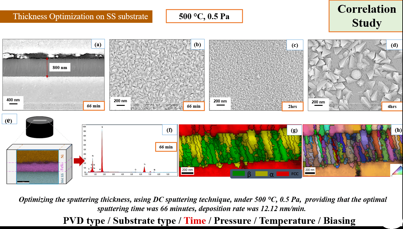
Thickness optimisation & correlation study (500 °C, 0.5 Pa): SEM, EDS and EBSD
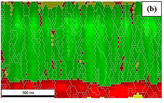
EBSD phase map: β 90% ± 10%, α 10% ± 5% (1 h, 500 °C, 1 Pa)
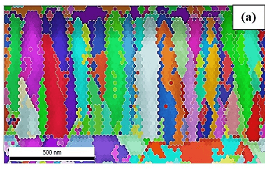
EBSD IPF map of columnar β-FeSi₂ grains
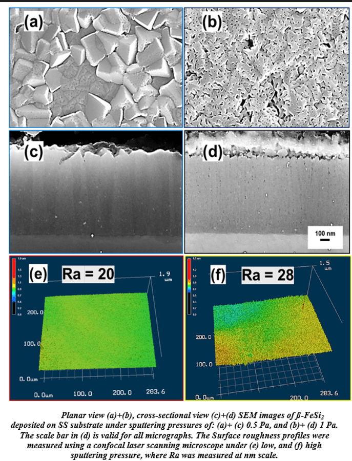
SEM plan and cross-section views and roughness profiles at 0.5 and 1 Pa

Methods & Materials

From process to microstructure

EBSD – Microstructure & texture
EBSD

Microstructure & texture

2D maps on cross-sections and plan views; spherical indexing for complex phases.

EDS · XRD – Composition & phases
EDS · XRD

Composition & phases

Elemental composition and phase identification of β-FeSi₂ formation.

SEM – Electron microscopy
SEM

Electron microscopy

Plan views and cross-sections of the films, thickness and morphology.

Materials & substrates

β-FeSi₂ thin films (~800 nm)DC sputtering (PVD)304 stainless steelSi (100)Sapphire Al₂O₃ (0001)Confocal laser microscopySpherical indexing

Projects

Further research projects

02Master’s research · KIT & JUST

Nanoengineering & Nanoscience

M.Sc. with distinction (2018–2020): MSM photodetector (Au/Pt Schottky electrodes on Si), MgF₂/TiO₂ anti-reflection coatings on GaAs (COMSOL) and sol-gel nanostructures (ZnO, Ag nanorods).

Mask aligner · sputtering · Keithley 4200A · COMSOL · SEM · UV-VIS
03Perovskite solar cells

Up-conversion Crystals for Perovskite Solar Cells

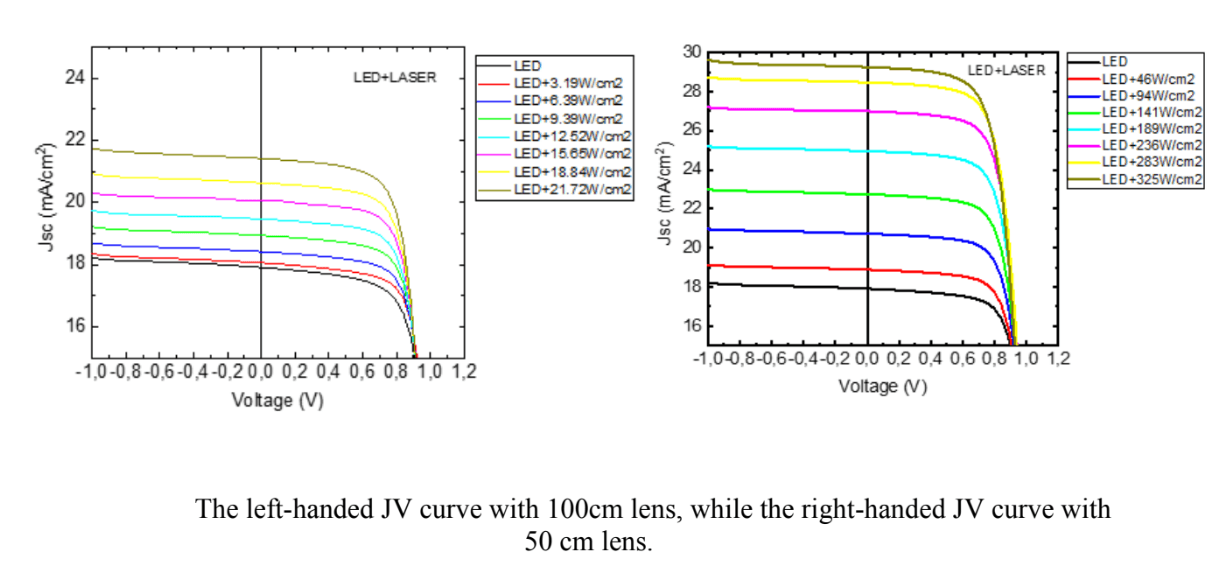
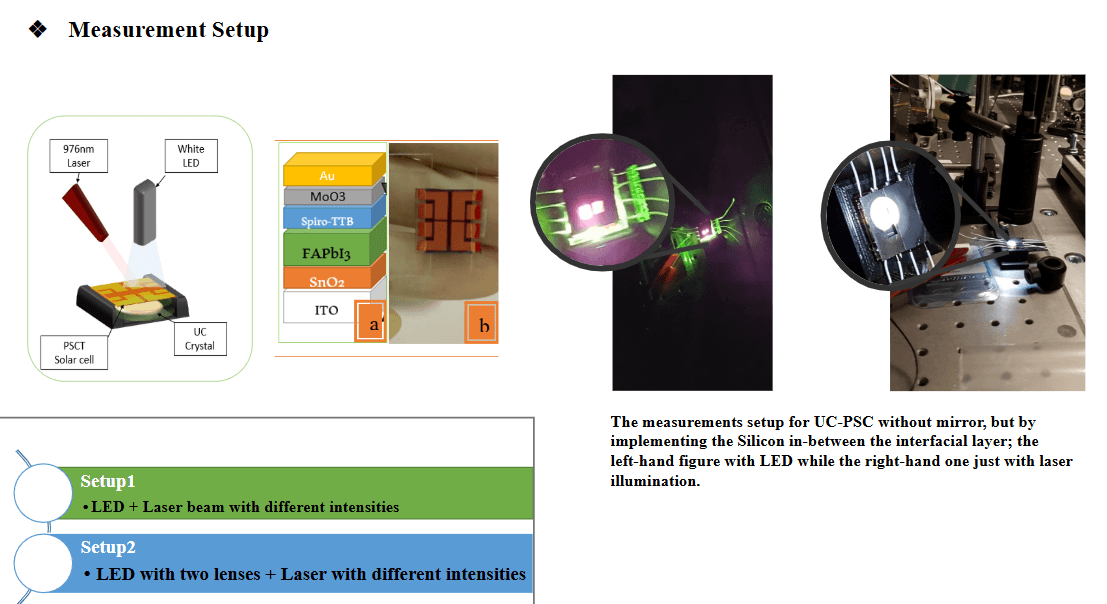
Modeling and Characterization of the Conversion Efficiency Enhancement of Perovskite Solar Cells that Employ Upconversion Crystals for the Solar Spectrum. UC crystals turn 976 nm light into visible light, so the cell harvests more of the solar spectrum.

~50%

more Jsc at maximum laser power

29.17 mA/cm²

Jsc with 50 cm lens (18.99 without)

+8.3%

Jsc gain predicted by the model

Best of 12 crystals: BaF₂ : 15% Yb³⁺, 2% Er³⁺ · FAPbI₃ cells · laser and LED setups

Up-conversion Crystals for Perovskite Solar Cells
J-V curves with 100 cm and 50 cm lens
04COMSOL simulation

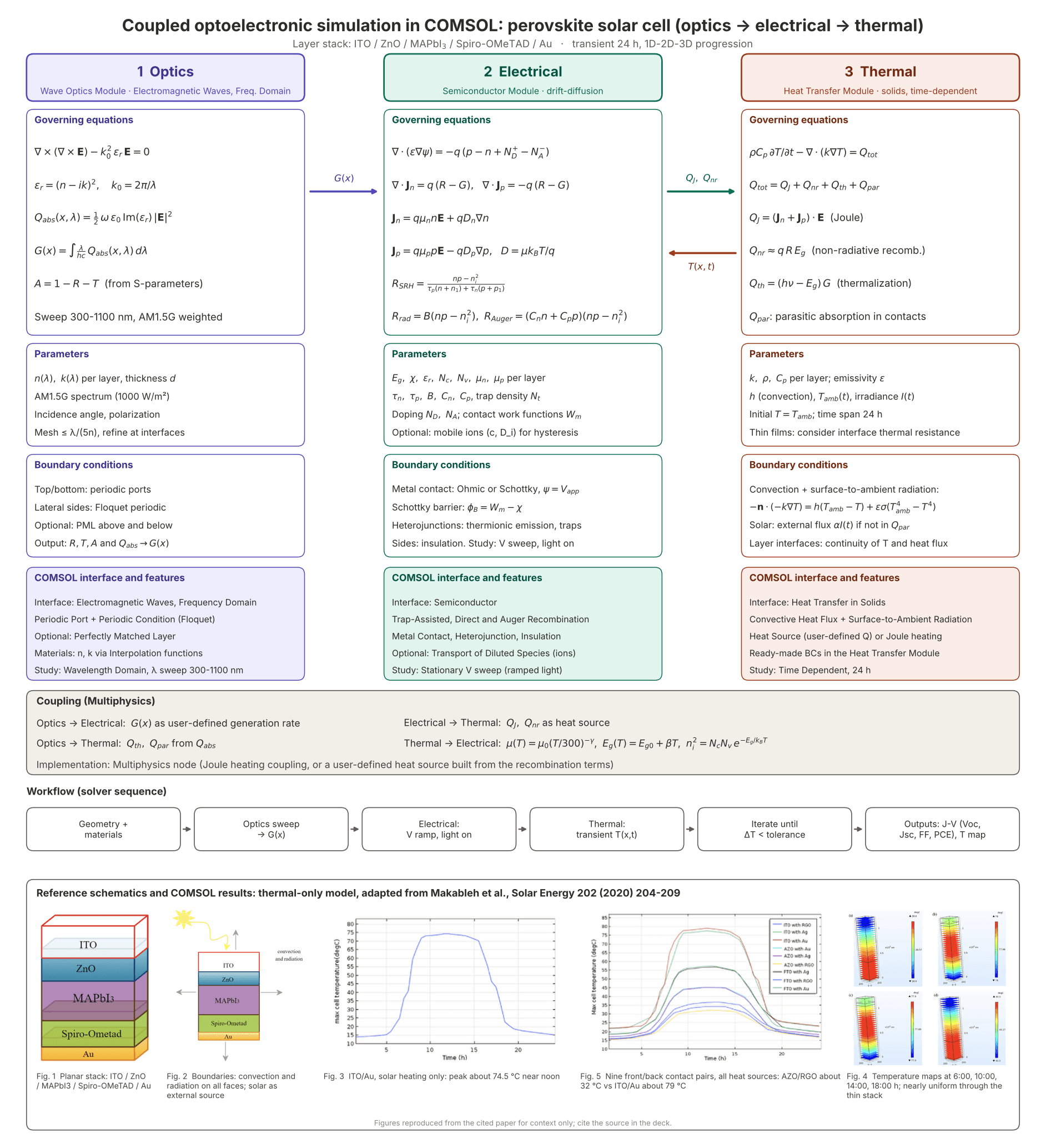
Coupled Optoelectronic Simulation of a Perovskite Cell

One model links light absorption, charge transport and heat in an ITO / ZnO / MAPbI₃ / Spiro-OMeTAD / Au stack over 24 h (1D → 2D → 3D): optics → G(x), drift-diffusion with recombination → J-V, heat transfer → T(x,t).

Wave Optics · Semiconductor · Heat Transfer · reference results after Makableh et al., Solar Energy 202 (2020)

Coupled Optoelectronic Simulation of a Perovskite Cell

Relevance to the Role

What I bring to process development

Process parameters → properties

I understand how deposition and process parameters shape material properties.

Temperature → microstructure

Hands-on experience of how temperature drives microstructure and phase evolution.

Experimental planning & analysis

Systematic design of experiments and structured analysis of large measurement data sets.

Data-driven troubleshooting

Troubleshooting based on data and evidence rather than assumptions.

My next development step

Industrial furnace and heat-treatment processes: I want to transfer my knowledge of temperature-dependent phase formation to industrial scale and keep growing in this area.

Experience

Career path

  1. Scientist

    07/2020 – present

    Max Planck Institute for Iron Research (MPIE) GmbH · Düsseldorf

    • Microstructure–property correlations and formation mechanisms of polycrystalline β-FeSi₂ thin films using correlative electron microscopy.
    • Fabrication via DC/RF sputtering; parameter optimisation for layer uniformity and adhesion with industrial relevance in mind.
    • Characterisation with EBSD, ECCI, cathodoluminescence and atom probe tomography.
    • Modelling of optoelectronic properties in COMSOL and MATLAB; predictive maintenance protocols for lab instruments.
    • Characterisation of perovskite solar cells for the University of Wuppertal.
  2. Laboratory Engineer

    01/2020 – 06/2020

    Karlsruhe Institute of Technology (KIT) · Karlsruhe

    • Fabricated perovskite solar cells in cleanroom and glovebox.
    • Boosted efficiency with up-conversion quantum dots; characterised with laser spectroscopy, XRD and Raman.
  3. Research Assistant

    06/2019 – 12/2019

    Al Hussein Technical University (HTU) · Amman

    • Research on smart energy systems and sustainable materials; coordinated inter-university collaborations.
  4. Research Intern

    07/2018 – 09/2018

    LMU Munich & TUM Open Research Lab · Munich

    • Developed the OSWD method to integrate organic semiconductors with graphene; analysis by STM/STS.
    • Presented the lab’s research at TEDxTUM.
  5. Head of Planning & Development

    01/2017 – 10/2017

    Power Guide for Energy Systems · Amman

    • Designed ground-mounted and rooftop PV systems for industrial, residential and agricultural clients; technical proposals and client negotiations.

Education

  • 2020 – 2025

    PhD in Materials Engineering (Dr.-Ing.)

    RWTH Aachen (research at MPIE Düsseldorf)

  • 2018 – 2020

    M.Sc. Nanoengineering & Nanoscience – with distinction

    KIT Karlsruhe & JUST

  • 2011 – 2015

    B.Sc. Electrical Power Engineering

    Al-Balqa’ Applied University

Core competencies

Materials & processes

PVD / DC & RF sputteringProcess optimisationMicrostructure–propertySol-gelCleanroom & glovebox

Characterisation

SEMEBSDECCICLFIBSTEMAPTAFMSTM/STSXRDRamanUV-VIS

Simulation & programming

COMSOLMATLABPythonC++AutoCAD

Energy & photovoltaics

Perovskite solar cellsβ-FeSi₂PV system designPVsystHelioScope

Selected Activities

Conferences, collaborations & initiatives

Conferences & presentations

  • IEEE-NANO 2024 – Gijón, Spain
  • MSE Congress 2022 – talk on β-FeSi₂ thin films
  • Solar Solutions Düsseldorf & Bremen (2023–2024)
  • TEDxTUM – lab representative (2018)
  • ICCNA (2018)
  • High Voltage Conference – speaker, University of Jordan (2014)

Workshops & collaborations

  • Perovskite characterisation with the University of Wuppertal
  • Thin-film training (DC/RF PVD), RWTH Aachen
  • FIB, 3D-SEM and SEM-CL training at MPIE
  • Graphene and STM research with LMU & TUM

Initiatives & engagement

  • IEEE / IEEE Women in Engineering
  • Association of Energy Engineers (AEE)
  • Jordan Engineers Association (JEA)
  • Science communication for broad audiences

MSE 2022 · Formation and characterization of β-FeSi₂ thin films for solar cell applications

What I took away

Presenting complex results clearly, working across research and industry, and coordinating international teams.

Awards

  • 2025

    CTCN MENA Youth Climate Innovation Award – 1st place

  • 2022

    CTCN MENA Youth Climate Innovation Academy Award – 1st place

  • 2018

    LMU Munich International Award – 1st place finalist

  • 2018

    TUM Open Lab Research Award

Publications

  • Greiner, A., Abu-Muhfouz, M., Guadarrama, A., Heckl, W. M., Trixler, F. – “Conducting Experiments with Organic Semiconductors: A Simple Sample Preparation for STM Courses”, J. Chem. Educ. (in preparation).
  • Rabady, R., Abu-Muhfouz, M. – “Modeling and Testing Efficiency Enhancement of Solar Cells Using Quantum Dots as Down-Converters”, Solar Energy (in preparation).

FAQ

Quick answers

Who is Dr.-Ing. Maram Abu-Muhfouz?+

A materials engineer with a PhD in Materials Engineering from RWTH Aachen and an R&D process engineer based in Düsseldorf. She researched β-FeSi₂ thin films for photovoltaics at the Max Planck Institute.

Which techniques does she master?+

Thin-film deposition (DC/RF sputtering, PVD) and characterisation with EBSD, XRD, SEM, ECCI, cathodoluminescence, FIB and atom probe tomography; simulation in COMSOL, MATLAB and Python.

Which roles is she open to?+

Process engineer, R&D engineer and materials scientist roles in industry and applied research – especially coatings, heat treatment, semiconductors and photovoltaics.

Which languages does she speak?+

German (C1), English (C1) and Arabic (native).

Contact

Let’s talk

Open to roles in process development and research & development. I look forward to hearing from you.

German C1 · English C1 · Arabic native